|
|
Single-Chip Passive UHF RFID Tags and Readers
|

Project Goal
The aim of this part of the project is the radio frequency identification (RFID) tag's power management integrated circuits. Various circuit topologies and ultra-low-power techniques will be investigated and developed.
Project Description
In this project, different power ICs will be developed to efficiently provide power supplies for the signal processing and memory circuits. Rectifiers, charge pumps, and, if necessary, voltage regulators will be studied and developed. Specific emphasis will be given to the optimization and ultra-low-power techniques of these circuits.
Faculty
Research Assistant
Yip Sum TSUI ( 徐 業 森 )
Jun YI ( 易 俊 )
Tracking Record and Accomplishment
|
Stage |
Milestone |
Status |
|
Phase I (May 1, 2005 – July 31, 2005) |
1) Study of prior power management schemes of RFID tags 2) Study of prior AC-DC multi-stage rectifier topologies |
Accomplished
Accomplished
|
|
Phase II (Aug 1, 2005 – Oct 30, 2005) |
1) Analysis of AC-DC multi-stage rectifier 2) Design of AC-DC multi-stage rectifier |
Accomplished
Accomplished
|
|
Phase III (Nov 1, 2005 – Jan 31, 2006) |
1) Analysis of AC-DC multi-stage rectifier 2) Layout and tape-out of AC-DC rectifier 3) Study of antenna / rectifier impedance issues |
Accomplished
Accomplished
On-going |
|
Phase IV (Feb 1, 2006 – Apr 30, 2006) |
1) Analysis, design, simulation and layout of high-voltage micro-power charge pump 2) Test of AC-DC rectifier 3) Study of antenna / rectifier impedance issues |
on-going
on-going on-going
|
|
Phase V (May 1, 2006 – July 31, 2006) |
1) Test of high-voltage micro-power charge pump |
|
|
Phase VI (Aug 1, 2006 – Oct 30, 2006) |
|
|
Design
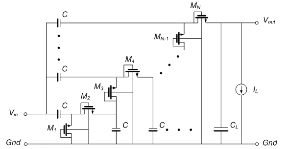
Multi-stage rectifier (rectifier and voltage multiplier combo)
Layout
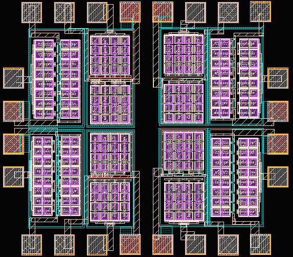
Layout of Multi-stage rectifier
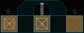
Layout of Test Structure
Simulation
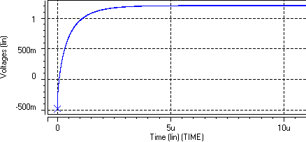
Post-layout simulated output voltage of the 16-stage rectifier.
Fabrication
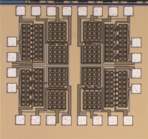
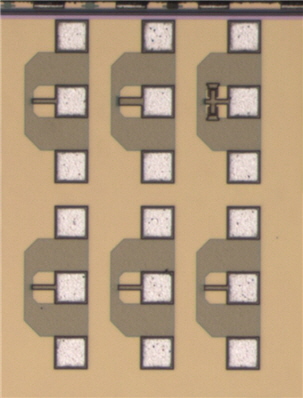
Die Photo of Multi-stage rectifier